Partner full and short name: Interuniversitair Micro-Electronica Centrum (imec)
imec is at the forefront of world-class research in nano-electronics and nanotechnology. imec’s research endeavors are concentrated in the realms of renewable energy, enhanced healthcare, intelligent electronics, and safer transportation. Our Photovoltaic (PV) division is dedicated to the advancement of cost-effective, scalable, and highly efficient solar cell technologies, with a primary focus on silicon-based and thin-film solar cells and modules. This research capitalizes on imec’s extensive semiconductor physics, processing, and analysis expertise. The Thin-Film PV group boasts a rich history spanning nearly two decades. Initially, our work centered on organic solar cells, but we have since shifted our primary focus to chalcogenide and perovskite thin-film solar cells. Notably, our perovskite thin-film solar cell research has garnered widespread acclaim due to its rapid progress. In recent years, we achieved a remarkable single-junction cell efficiency of 24.3% for inverted p-i-n cells using a stable and scalable layer stack. In 2017, we proudly secured the world-record-certified module efficiency of 12.5%. In 2018, we achieved another breakthrough by introducing the world’s first 4 cm² module-on-cell perovskite/silicon stack with a power conversion efficiency of 25.3% (27.1% at the cell-on-cell level), surpassing standalone silicon solar cells. imec has successfully demonstrated modules with efficiencies of 16.3% and 13.1% for areas of 100 cm² and 784 cm², respectively. The imec PV group has dedicated state-of-the-art processing facilities (1500 m²) in EnergyVille available for the fabrication and characterization of thin-film and silicon devices and modules. There is a spin coating platform for screening materials and cell design at laboratory device scale up to 5×5 cm2, and a blade coating platform for fabrication of intermediate-size perovskite minimodules up to 15×15 cm2. A perovskite assembly line allows to process of modules up to 30x30cm² on 35×35 cm2 substrate in controlled atmosphere gloveboxes. Slot-die coater, vacuum thermal evaporation, and sputtering systems allow for relevant coatings. A 3-wavelength picosecond laser is available for the creation of module interconnections.
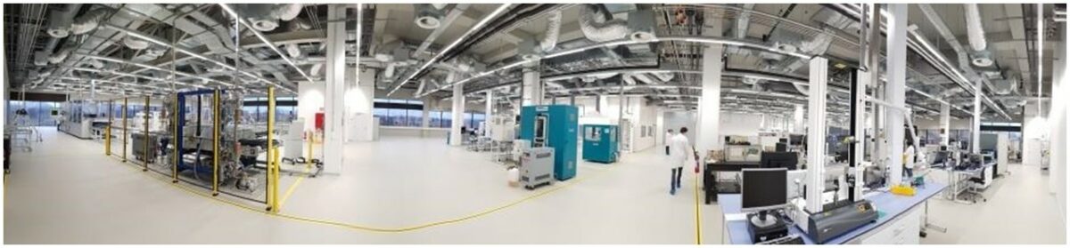
Photo: View on 1500 m² PV module, battery, and TF-PV facilities in EnergyVille, Genk, Belgium
More details on imec TFPV lab https://www.energyville.be/en/labs/thin-film-pv-lab
Main tasks and responsibilities within the project:
In this project, imec will mainly contribute to research excellence and training of young researchers. Specifically, imec will organize on-site visits of researchers from partners, at least 2 people per project year. Training of researchers on the fabrication and characterization of perovskite photovoltaic devices will be carried out at imec. Exchange PhD students from FORTH to imec for a short-term internship could also be arranged. imec will also be involved in webinars, virtual meetings, and guest lectures at FORTH and other partners.