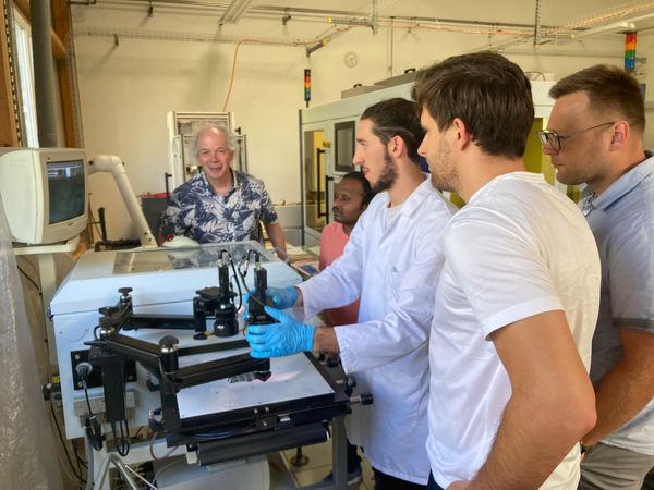
During this visit, our team:
1. Had the opportunity for an on-site demonstration of the implemented research activities of the researchers involved in the APPROACH project.
2. Exchanged ideas on potential materials needs for specific applications such as highly-conductive materials with tailorable semi-conducting behavior, and, environmentally friendly, and scalable reproducible inks for films fabrication.